 Creating an XSA for STYNQ
Creating an XSA for STYNQ
Creating an XSA for STYNQ
STYNQ doesnt use Board Support Packages -- it derives everything from the XSA file. Thus it is critical that the XSA file be correct for your board. The XSA is created by Vivado from the Block Design in your project. In that design, the configuration of the Zynq processor block is especially important, since it specifies which pins and clocks the board uses for many of the PS devices, such as serial ports, ethernet, USB, DisplayPort, and PCIe.
The configuration in the Block Design is put into the XSA file, and this is used to create proper boot files and to specify to the Linux kernel how to properly configure devices.
The XSA file also has information about user devices configured into the PL. These are not used by STYNQ to configure any boot files or the Linux kernel, since STYNQ boots the PS first into Linux and then configures the PL from Linux. So at boot time, PL devices aren't present.
However, C++ programs running under Linux do need to know what devices are in the PL after it is loaded. For this, STYNQ provides a utility to convert the information in the XSA into C++ files that describe the PL to C++ programs.
The following discusses how to properly configure the ZYNQ processor block in Vivado, using information from the schematic diagrams of a board. This procedure is intended to work for any board using a ZynqMP for which you have a schematic diagram. To clarify each step, an example will be given of how that step would be done for the RFSoC4x2.
Configuring the ZYNQ block is best done through the Vivado GUI.
First, the Vivado project needs to be for the correct ZynqMP FPGA that's on the target board. Verify this is correct on an existing project, and if not change it. Alternately, start a new project with the correct FPGA.
You can usually find the exact FPGA part number from the board schematic. For example, search the schematic for "XCZU", the starting characters of a Zynq FPGA designation. If you do this for the RFSoC4x2 schematic, you quickly find that it is the XCZU48DR-1FFVG1517E FPGA. Start Vivado, select "Create Project", Select an RTL project with no souces, and search for this FPGA. You'll find it doesn't exist in Vivado. Searching for just "xczu48dr" gives some options, and we can find the xczu48dr-ffvg1517-1-e. It appears to be the same part, with just the numbers in a different order. Select it. Because the match isn't exact, it may be best to also confirm it's correct with another source, such as other board documentation. Then finish creating the new project.
In this empty design, create a Vivado Block Design with "Create Block Design" in the left panel. In this block design, click the large + to add IP. Search for "Zynq", and add "Zynq Ultrascale+ MPSoC". Double-click on the Zynq block to start configuring it.
Here is how one would configure the I/O interfaces for an RFSoC4x2. On the left, click on I/O configuration. For the I/O configuration, the top item is the MIO Voltage Standard. This can be found by finding the MIO bank on the schematic and finding what voltage it is powered with. Bank 1 in the Vivado configuration is often called Bank 501 on the schematic. Bank 2 is 502. Etc. Find the power pins for that bank, and set the voltage accordingly. The voltage can also be found from the schematic by finding one of the MIO pins in the selected MIO bank and following it to see what it is connected to. If the device it is connected to has 1.8V VCC, then use LVCMOS18. If the VCC is 2.5V, use LVCMOS25. If the VCC is 3.3V, use LVCMOS33. It can also be found by finding the VCC pins for that bank on the Zynq processor connections on the schematic. The last MIO bank, Bank3, is simply called "Dedicated" in the Zynq processor configuration. This is where the PS JTAG and PS REF CLK are connected. The voltage of devices connected to these pins can be used. For the RFSoC4x2, the schematic sheet titled "PS: BANKS 500-502" shows that Bank 0 uses 3.3V, and Banks 1 and 2 use 1.8V. Set the voltage standard to match. The sheet titled "RFSoC Config" shows that Bank 3 also uses 1.8V.
Next click on the arrow to the left of "Low Speed" in the I/O configuration to see possible low-speed interfaces. First is "Memory Interfaces", and first of these is the QSPI. Searching for QSPI shows nothing on the RFSoC4x2 schematic. Searching the web shows that this is an interface for Flash memory. Searching the schematic for "Flash" also finds nothing. We leave this interface unconfigured. It may be that this board has no flash memory. Regardless, STYNQ boots from a microSD, not flash memory, and flash isn't used for anything else. So a flash memory device could be omitted even if it's present. Greater certainty about whether this device is on this board could be had by enabling the QSPI interface. Once enabled, the I/O configuration window allows MIO pins to be selected. The choices are limited. The schematic can be searched to trace each of these pins to see to what device they actually connect. If none connect to a Flash Memory device, you can be sure that there is none on the board. If some do connect to a flash memory device, that information is used to configure the I/O.
Next is "NAND". This can remain unconfigured, for the same reasons.
Next is "SD". This is the microSD card interface. There are two options, SD0 and SD1. Typically, only one is used by a board. If you enable SD0, you can look at the pulldown menus to find that it uses EMIO, MIO 13-22, MIO 38-48, or MIO 64-74. SD1 uses EMIO or MIO 39-51. You could search for these MIOs in the schematic, although it may be quicker to search for "sd card", which is on sheet 12 of the RFSoC4x2 schematic. This shows MIOs used are 13-16, 21, 22, 24, and 25. This is clearly SD0, so configure it with the correct MIO pin range in the I/O congfiruation. Looking more carefully at the schematic, MIO 24 is used for SD Card insertion detect, which is not part of the normal SD Card interface. Similarly, MIO 25 is used for write protect functionality. Since these are connected, enable them.
Next, move on to I/O Peripherals: CAN, I2C, PJTAG, PMU, CSU, SPI, UART, and GPIO. Of these, only the UART needs to be configured for STYNQ. The I2C and SPI may need to be configured if you're using some Xilinx drivers.
For the RFSoC4x2 board, Sheet 7 of the schematic shows that UART0 is used, connected to MIO 32 and MIO 33. Note that UART0 in the Vivado Zynq I/O configuration does not allow MIO 32/33 as an option. UART1 does. So what is called UART0 on the schematic is actually UART1 in the Zynq configuration. There are additional UART settings, such as whether it's CMOS, the drive strength, the slew, and the pullup. For the RFSoC4x2, the UART pins go to a USBSerial chip, so drive strength required should be minimal. Speed shouldn't be an issue. Nevertheless, I left these at default values. This may use slightly more power. The modem isn't necessary.
The RFSoC4x2's Sheet 20 shows the I2C connecting to MIO 36 and 37. The Zynq I/O configuration shows this is possible by enabling I2C 1. It also shows I2C on MIO 18 and 19. Selecting these MIOs for the I2C indicates a conflict with the SD card interface, using MIO 13-22. This is resolved by going to the SD Card interface and changing it to SD 2.0 from SD 3.0. The 2.0 interface uses less pins.
The RFSoC4x2's Sheet 20 also shows the SPI interface for the OLED on MIO 6, 9, 10, and 11. This is available by enabling SPI 1.
Other low-speed interfaces can remain unconfigured for STYNQ.
High-speed interfaces in the I/O configuration are GEM (Ethernet), USB, PCIe, DisplayPort, and SATA. Of these, GEM, USB, and DisplayPort are on the RFSoC4x2 board.
The GEM Ethernet I/O can be seen on Sheet 20 of the RFSoC4x2 schematic diagram. It shows MIO 38-51, and MIO 26 for a reset. This is GEM1, which is then enabled in the I/O configuration. There is also configuration for an "External TSU Clock". TSU apparently stands for "Time Stamp Unit". This should be disabled.
There are two USB interfaces on the RFSoC4x2, one master/host and one slave. For STYNQ, only the master need be configured. It uses MIO 64-77, which is USB1. Furthermore, it can be configured for USB 3.0, which also uses a GT lane. Sheet 22 shows that the correct GT Lane is Lane 3.
The DisplayPort uses MIO 27-30 (From Sheet 20). It uses GT Lanes 0 and 1 (From Sheet 22). (This is "Dual Lower" on the I/O configuration.) The DPAUX pins may need to be set to CMOS and FAST. I ran into some trouble where they were incorrectly set. Also, When changing them their configuration disappeared. If this happens to you, click OK to save the one you changed, then close the Zynq configuration and reopen it. You should now be able to see the settings again, and change the next one.
There are two possible Reference Clocks in the I/O configuration, the VIDEO REF CLK and the PCC ALT REF CLK.
The VIDEO REF CLK can be configured to either MIO 27 or MIO 50. Searching for "MIO27" in the schematic shows that it is already used for a different purpose by the DisplayPort. Searching for MIO50 shows that it is used by the GEM Ethernet. So this should not be configured.
The PCC ALT REF CLK can be configured to MIO28 or MIO51. These conflict with the DisplayPort and the GEM Ethernet, respectively, and thus this should not be configured.
Clock Configuration has two tabs at the top, "Input Clocks" and "Output Clocks".
Input Clock Configuration has three items, "Input Reference frequency", "GT Lane Reference frequency", and "Peripheral Reference frequency".
This has a single frequency entry, the PS_REF_CLK frequency. Searching for ps_ref on the schematic finds it on Sheet 15, which shows it has a frequency of 33.33MHz.
There are two frequencies here for the above configuration, DisplayPort and USB1.
DisplayPort can use one of four Reference Clocks and one of three frequencies for that clock. Searching for "27 mhz" in the schematic shows that it is indeed set for 27MHz of the three possible selections, on the signal GTR_505_REF_CLK_DP. Searching for this pin shows that it is connected to the MGT Ref Clock 0, on Sheet 22. Note that when selecting the "Source" Ref Clk, the selection box may be too small to see which reference clock number is selected. The box may need to be resized to show this information.
USB1 can use one of four Reference Clocks and one of three frequencies for that clock. On Sheet 15, it shows GTR_505_REF_CLK_USB3 at 100MHz. Searching for this pin shows it is connected to MGT Ref Clock 1, on Sheet 22. Note that the name "USB3" on this pin probably refers to it being for USB3.0 support -- it isn't associated with the Ref Clock number or with the USB device number.
With the configuration above, this has no items to configure.
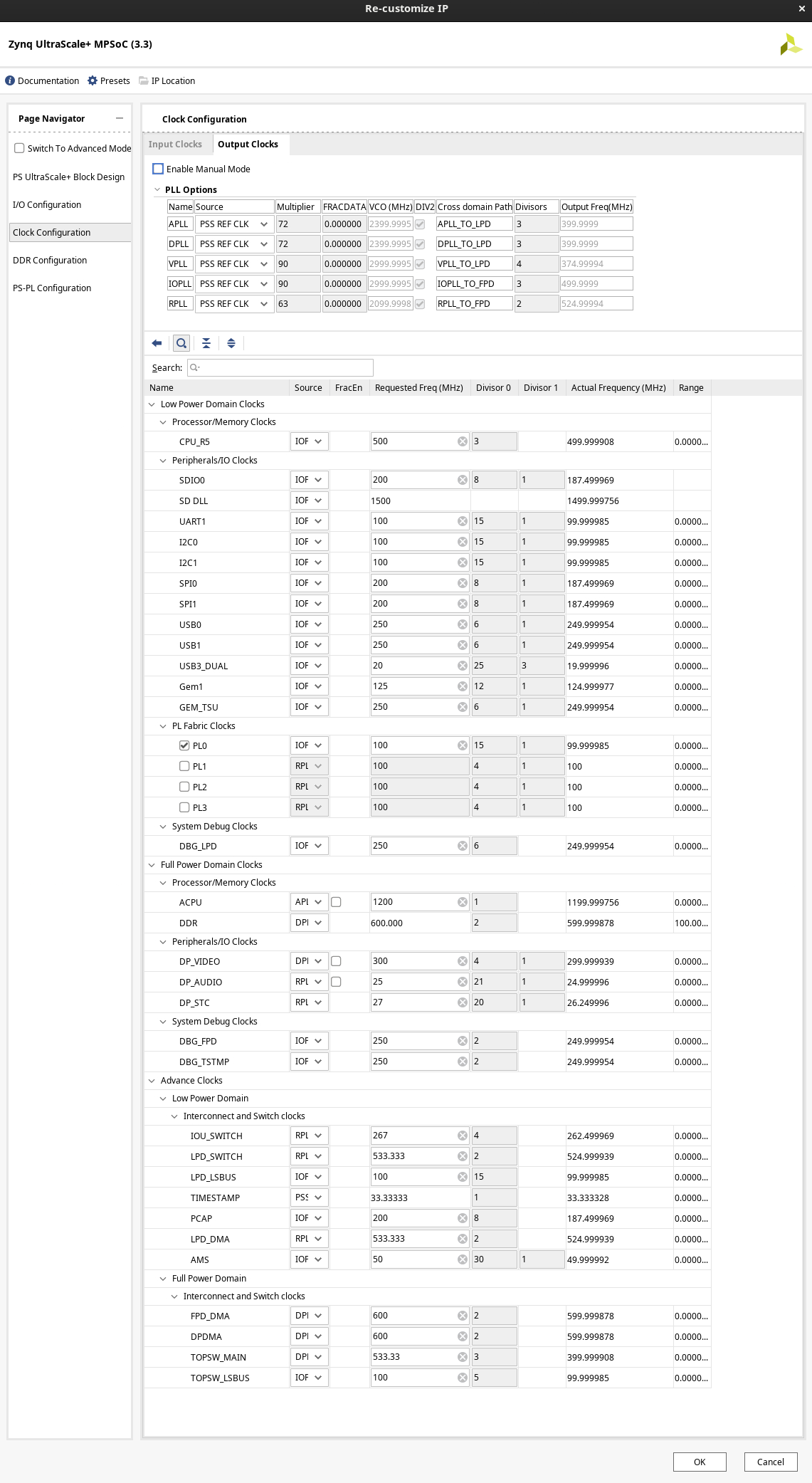
Output clock configuration is a matter of selecting PLL frequencies for a selection of PLLs at the top, and then selecting which clocks are derived from them at the bottom. This is confusing to me. For example, some documents state that the DP_VIDEO clock should be on the VPLL, with nothing else connected to it, so that the DisplayPort driver in Linux can set its frequency appropriately. However, doing this seems to make the DisplayPort video unstable, in my experimentation. Also, it's not clear to me what all the considerations are in deriving these settings. With some experimentation and reference to other designs, I found settings that seem to work for me. A picture of them is here:
DDR pins are found on the RFSoC4x2 Schematic Sheet 32. This shows the part number for the DDR4 is MT40A512M16LY-062E. Searching for this part on the web finds a datasheet from its manufacturer, Micron.
The DDR4 datasheet shows that the -062e part is DDR4-3200. The tooltip for DDR4 Speed Bin shows that DDR4-2400 is the max supported by the FPGA. So I'll treat this fast DDR-3200 chip as if it's the slower speed -083e DDR4-2400 chip described in the DDR4 datasheet. Note that other RFSoC4x2 documentation does specify the -083e part. Perhaps it was replaced for extra timing margin or due to part availability.
Typically put the Requested Device Frequency at the maximum for best performance. This is 1200MHz.
The memory type is clearly DDR4. It's an on-board component, so Components is set to Components. The Effective DRAM Bus Width is 64 bits, shown as on the RFSoC4x2 schematic sheet 34, with data bits PS_DDR4_DQ0 through PS_DDR4_QD63. This is not an ECC part. (No mention of ECC on the DDR4 datasheet or RFSoC4x2 schematic.)
For Speed Bin, the max supported in the Zynq DDR Configuration is DDR4-2400. This is a DDR4-3200 part, from its datasheet, but there are similar parts on the datasheet that are slower versions with slower timing. The -083e version of the chip is DDR4-2400, so I'll treat this part as that slower part. The tooltip for "Speed Bin" shows that "DDR4 2400R" has timing 16-16-16. These numbers are CAS Latency (CL), Row Column Delay (tRCD), and Row Precharge Time (tRP). I'll choose this, since the -083e version of this DDR4 has CL=16, nRCD=16, and nRP=16. (From the DDR4 datasheet, Table 1.)
CAS Latency is referred to as "CL" in the DDR4 datasheet. As mention above, it is 16 cycles. RAS to CAS Delay is tRCD, which is 16 cycles. Precharge time is 16 cycles.
t_RC can be found from the DDR4 datasheet, Page 314 Table 160, "DDR4-2400 Speed Bins and Operating Conditions". It shows t_RC as t_RAS + t_RP, with t_RAS=32ns and t_RP=13.32ns (Minimum). So a minimum value for t_RC is 45.32ns.
t_RASmin is 32ns, per the paragraph above.
t_FAW depends on the page size. The page size of the DDR4 is 2KB, per Table 2 on page 2 of the DDR4 datasheet. Page 328 of the datasheet shows that for a 2KB page size with DDR4-2400, tFAW is a minimum of 30ns.
DRAM IC Bus width per die is 16. (4 dies make up the 64-bit effective bus width.) This is shown on the RFSoC4x2 Schematic, sheet 32.
DRAM Device Capacity per die is 8Mbits, from the DDR4 datasheet. Bank Group Address Count is 1 bit, from the DDR4 datasheet. Similarly, Bank Address Count is 2 bits, Row Address Count is 16 bits, and Column Address Cpount is 10bits. These can all be found from Table 2 of the datasheet on Page 2.
Once all the DDR configuration is done, a good double-check is that at least the memory size is right. The PS memory on this board should be 4GB, and that matches the "DDR Size" value in the lower right corner.
Under the assumption that these settings are unusual and don't typically require changing, I left them alone.
STYNQ doesn't typically need much here, but is OK with anything that you want to do for your design. Everything can be disabled, except the "Master Interface" "AXI HPM0 LPD", which is the primary AXI bus for the PS to control the PL. It is probably best to leave it at 32 bits wide. These settings are the default.
Now that all settings are complete, click "OK" at the bottom right of the window. This saves the settings.
In the block Diagram window, the Zynq block should have one input, a clock pin maxihpm0_lpd_aclk. This needs to connected to the output clock pl_clk0, to indicate which clock is used for the AXI bus.
This Zynq block can be the only thing in the project for purposes of generating BOOT.BIN, BOOT.SCR, and the linux device tree. Alternately, a full design can be present. The boot files will be the same either way. Any PL devices that are present will be omitted from configuration of the boot files, so that Linux can boot without the PL loaded.
Next, the Block Design must be "generated", via the "Generate Block Design" action under "IP Integrator" on the left sidebar in Vivado.
Then do File -> "Save Block Design".
For a new design only, find the "Sources" tab by selecting Window -> Sources. In its list you should see the "bd" file, design_1.bd. Right-click on it, and select "Create HDL Wrapper". It may ask to let Vivado manage the wrapper. This can be done either way, depending on how you would like to do future projects. If you want to add IP at the top level, Vivado shouldn't manage the top level. If you want to add all IP from within the IP Integrator's block design, then perhaps Vivado should manage the top level.
Next do File -> Export -> "Export Hardware". This creates an XSA file that describes the Zynq configuration, and is used by STYNQ to create the BOOT.BIN, BOOT.SCR, and device tree files. A bitstream should not be included; under STYNQ these are loaded separately.
The project should have automatically saved. Close it out with File -> "Close Project". Exit Vivado.
If all projects use the Zynq configured exactly the same, they can all use the same BOOT.BIN, BOOT.SCR, and linux device tree, and PL for those projects can be loaded and changed out at run time. So whenever starting a new project, it may make things easier to copy this project as the base.
XSA files are ZIP format files. You can unzip them to see the contents. There is an entire HTML file in there that you can open to see how it specifies that things are configured. There is specific initialization code that ends up being compiled into the BOOT.BIN file. There are data files that specify the system devices, and are used to create the device tree. There is a Hardware Handoff file, HWH, which specifies all of the details of the devices. STYNQ expects you to put this XSA file into the STYNQ_BASE/boot/inputs/XSA directory to build boot files, if a previous XSA doesn't have the same ZYNQ configuration to use the same boot files. To create C++ header files to drive the PL devices, put the XSA into the STYNQ_BASE/xsa_to_c++/inputs directory. Then run the build.sh process to create outputs in the respective "out" directories.